Docket #: S25-163
Diffraction-Based Electron Beam Lithography for Chip Manufacturing
Stanford researchers have developed a wide-area electron beam lithography (EBL) approach that combines the resolution of electron beams with the large-area exposure of conventional photolithography.
EBL can match or exceed the resolution of the most advanced extreme ultraviolet (EUV) tools, but it writes patterns one point at a time, which is too slow for integrated circuit mass production. Absorption-based masks that could pattern many features at once suffer from mask heating, degraded resolution, and impractically thick materials.
This method sends a high-coherence electron beam through a thin patterned mask that redirects electrons instead of stopping them. The mask stamps its pattern onto the beam while absorbing minimal energy. Electron optics then shrink the image onto the resist in a single wide-area exposure. Since the optics shrink the image, the masks can be made with standard microfabrication techniques. The approach builds on beam-shaping techniques first developed to generate coherent x-rays in free-electron lasers.
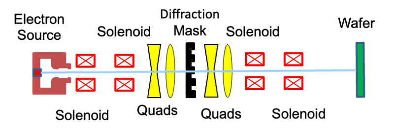
Schematic: Phase and Diffraction Contrast Imaging Based Electron Beam Lithography
(Image courtesy Emilio Nanni, Charlotte Wehner)
Stage of Development: Proof of Concept
The underlying beam-patterning method has been demonstrated experimentally, with full contrast over micrometer-scale areas.
Applications
- Lithography tools for high-volume semiconductor and integrated circuit manufacturing
- Next-generation patterning beyond the resolution limits of EUV lithography
Advantages
- Resolution about 100X finer than the best EUV tools and limited only by resist performance
- Throughput matching EUV through wide-area (millimeter-scale) exposure at high projected dose rates
- Compact and more efficient system with an estimated ~100X lower power than an EUV system at comparable throughput
- Durable masks made with standard, commercially available microfabrication processes
Related Links
Similar Technologies
-
High-Efficiency, Low Voltage Stress Power Amplifier with Push-Pull Wave-Shaping Operation S20-045High-Efficiency, Low Voltage Stress Power Amplifier with Push-Pull Wave-Shaping Operation
-
Novel Semiconducting Materials for High Brightness and Air Stable Photocathodes S21-100Novel Semiconducting Materials for High Brightness and Air Stable Photocathodes
-
Enhanced photoelectron sources using electron bombardment S13-018Enhanced photoelectron sources using electron bombardment